Naming and Standard-Setting
Naming and Standard-Setting: Teliang's First-of-its-Kind "PCB Stamped Welding Terminal" Reconstructs Industry Perception
Throughout the century-long development of the global terminal block industry, product naming has always played a core role as an "identity marker". A precise name can not only clearly convey the product's manufacturing process, application scenarios, and core characteristics but also promote industry-wide technical exchanges and standardization. However, when Teliang's R&D team was reviewing the global terminal block product system, they found that a core product widely used in fields such as photovoltaic inverters, energy storage BMS, and industrial control had long been facing the industry-wide dilemma of ambiguous naming. Traditional terms like "PCB screw terminal" and "PCB welding terminal" either confused connection methods or lacked crucial process information, leading to customer selection confusion and increased industry communication costs.
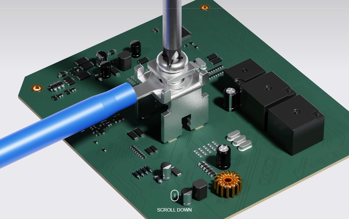
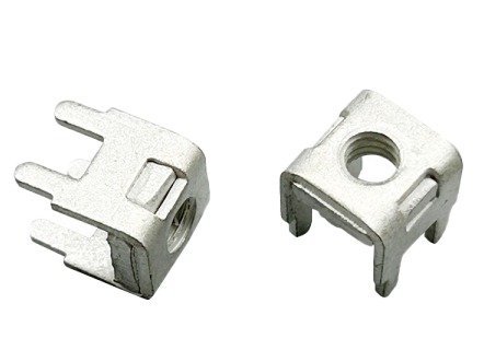
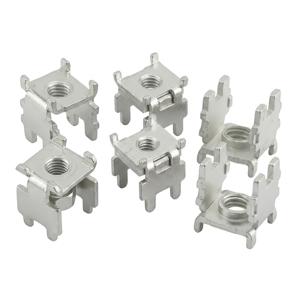
Based on a deep deconstruction of the product essence and accurate insight into industry pain points, Teliang officially named this type of terminal, which is "manufactured by stamping, applied to PCBs, fixed by welding, and used to connect wires", as the PCB stamped welding terminals, establishing new industry rules with professional naming and reshaping product perception with technological definitions, injecting new impetus into the standardized development of the global terminal block industry.
Industry Pain Points: The Ambiguous Dilemma and Perceptual Deviation of Traditional Naming
As the core component of electrical connections, the naming logic of terminal blocks should follow the core principle of "manufacturing process + application scenario + connection method" to ensure accurate and efficient information transfer. However, in the actual market, the naming of welding-type terminal blocks for PCBs has long been in a state of chaos. The two traditional terms both have significant flaws, becoming hidden barriers to industry development.
"PCB welding terminal" ignores the most crucial manufacturing process—stamping. The precision of the stamping process directly determines dimensional tolerance, electrical conductivity, and mechanical strength. The absence of this attribute allows low-end products made by casting to disrupt the market. On the other hand, "PCB screw terminal" creates a perceptual deviation, as "screw" implies a fastening method, whereas PCB stamped welding terminals rely on welding for fixation. This confusion increases communication costs and wastes project time, as seen in recent Turkish government projects where clarified requirements only emerged after three rounds of testing.
"PCB welding terminal" is the most commonly used term in the market at present. This name only clarifies two elements: "applied to PCBs" and "connected by welding", but ignores the most crucial manufacturing process of the product - stamping. In fact, the key components of this type of terminal, such as the conductive body and contact structure, are formed through precision stamping. The precision of the stamping process directly determines the dimensional tolerance, electrical conductivity, and mechanical strength of the terminal. The absence of the core attribute of "stamping" not only prevents customers from judging the manufacturing level of the product through the name but also allows some low - end products made by casting or turning processes to pass off as genuine, disrupting the market order. The purchasing manager of a Shenzhen - based photovoltaic inverter company once feedbacked to Teliang: "Due to the confusion caused by the name 'PCB welding terminal', we mistakenly purchased terminals made by the casting process. Their dimensional deviation exceeded 0.1mm, and after welding, there were problems with poor contact, resulting in the rework of the entire batch of products."
In addition to the confusion in customer selection and communication, ambiguous naming also restricts the unification of industry technical standards. Currently, the global terminal block industry has not yet formed clear classification standards for this type of product. The product parameters and performance indicators of different enterprises lack a unified reference benchmark, which is not only unfavorable for the product integration of downstream enterprises but also hinders industry - wide technological iteration. As a top - tier enterprise in the Dongguan terminal block industry, Teliang deeply realizes in the process of serving leading photovoltaic and energy storage enterprises in the Shenzhen - Dongguan region that standardizing product naming is not only a need for the company's own development but also a responsibility to lead the industry towards standardization and normalization.
Naming Logic: Three Core Elements Constructing a Precise Product Identity
The new name proposed by Teliang is based on a deep deconstruction of product essence, following a four-dimensional logic: "manufacturing process + application scenario + connection method + functional positioning"., achieving the complete transfer of product information. Each keyword carries clear technical connotations.
- Stamped (冲压): Precisely locks in the manufacturing process. Teliang's PCB stamped welding terminals are formed through precision stamping dies with tolerances within ±0.01mm, ensuring dimensional consistency far superior to casting.Compared with the casting process, the material utilization rate of the stamping process is increased by more than 30%, the production efficiency is increased by 5 times, and it can effectively avoid defects such as pores and cracks generated during the casting process. Incorporating "stamped" into the name not only showcases the manufacturing process advantages of the product but also provides customers with a core basis for quickly judging product quality.
- PCB: Clarifies the core application scenario. The size, spacing, and length of the pins are specifically adapted to PCB pad layouts for automated wave or reflow soldering.Its application scenarios cover multiple core fields such as photovoltaic inverters, energy storage battery BMS, industrial energy storage control systems, and photovoltaic combiner boxes, and it is a key component for electrical connections in new energy and industrial control equipment. Clearly defining the "PCB" application scenario helps customers quickly locate the applicable range of the product and improve the selection efficiency.
- Welding (焊接): Defines the connection method, ensuring stability under high current and high-frequency vibration.The connection between the wire and the terminal also relies on welding to ensure connection stability under harsh working conditions such as high current and high - frequency vibration. Compared with screw fastening, welding connection has advantages such as low contact resistance, strong shock resistance, and small space occupation, making it the preferred connection method for high - end new energy equipment. The clear indication of "welding" avoids confusion with screw - type terminals and allows customers to intuitively understand the installation process requirements of the product.The design of the welding pins is adapted to the automated welding process, and the welding qualification rate can reach over 99.8%.
- The organic combination of the three core elements constitutes the complete naming logic of the "PCB stamped welding terminal", not only achieving the accurate transfer of product information but also establishing clear product boundaries. This enables customers to quickly judge the manufacturing process, application scenario, and connection method of the product through the name, completely solving the ambiguous dilemma of traditional naming. This naming logic has also been recognized by industry experts. An expert from the Connector Branch of the China Electrical Equipment Industry Association said: "The naming of 'PCB stamped welding terminal' proposed by Teliang conforms to the classification principles of terminal block products, fills an industry gap, and provides an important reference for the subsequent formulation of industry standards."
The Path from Enterprise Identity to Industry Standard Leadership
Teliang's naming of PCB stamped welding terminals has far-reaching significance. At the brand level, it binds Teliang’s process advantages (30% market share in the Shenzhen-Dongguan region) to exclusive labels. At industry events like the Canton Fair, this professional naming immediately attracted overseas customers from Australia and Brazil.
At the market - competition level, the new name constructs a differential competition barrier. Currently, competition in the terminal block market is becoming increasingly fierce, and product homogenization is serious. A standardized and precise product name has become an important means of differential competition for enterprises. The naming of "PCB stamped welding terminal" enables Teliang to establish a professional advantage in the customer - selection stage. Customers can clearly understand the core advantages of the product through the name, thus standing out in the competition. At the same time, the new name also sets an implicit threshold for industry entry, forcing other enterprises in the industry to improve their manufacturing processes and product quality, promoting the market to develop in the direction of high - quality and standardization. The person in charge of a Dongguan - based energy - storage terminal block enterprise said: "Teliang's new name has made us realize that relying solely on low - price competition is no longer tenable. We must strengthen stamping process research and development and improve product precision to keep up with the development pace of the industry."
At the industry level, Teliang collaborated with leading PV and energy storage enterprises to formulate the "Technical Specifications for PCB stamped welding terminals," providing a unified reference benchmark. This has been recognized by international energy experts as a contribution to the standardized integration of global new-energy equipment.
Future Prospects: Leading the Global Industry Upgrade
With the global market for these products forecast to exceed $8 billion by 2030, Teliang will continue to iterate the stamping process with AI-vision inspection to push tolerances to ±0.005mm. By relying on the "Dongguan Manufacturing + Jiangsu Export" twin-pole layout, Teliang will bring Chinese-standard PCB stamped welding terminals to global clean energy projects, fulfilling the mission of "customer problems are innovation propositions."From ambiguous naming to precise definition, from enterprise identity to industry standard, Teliang has written a new chapter in leading the industry development with the naming innovation of "PCB stamped welding terminal". In the wave of global energy transition, Teliang will continue to adhere to the concept of "quality - oriented, innovation - driven", taking precise naming as the foundation and core technology as the wings, enabling Chinese - intelligent - manufactured terminal products to go global, providing solid connection support for the high - quality development of the global new - energy industry, and engraving the power of Chinese brands on the global terminal - block industry map.
What Is a Terminal Block What Is a Terminal Block Used For
Teliang Leads the New Track of Terminal Blocks
Related Article